


Technology
China's automotive chip race: From dependency to domestic innovation
Read more

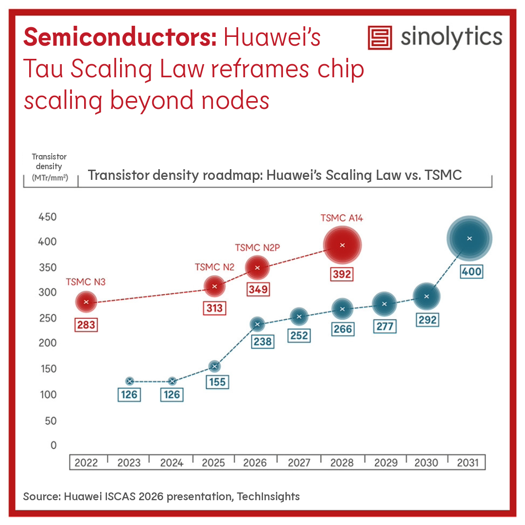
For decades, chip performance improvements largely came from making transistors smaller: the famous Moore's Law. Huawei's Tau Scaling Law points to a different path: optimizing across devices, circuits, chips, and systems together to reduce the time constant (τ), thereby boosting performance, energy efficiency, and transistor density. Put simply, it tries to make signals move through the chip faster and coordinate more efficiently, so the system can do more work in the same amount of time. Huawei says it has designed and mass‑produced 381 chips over the past six years based on this approach, suggesting the concept has moved from theory to products and mass production. According to Huawei's roadmap, by 2031, high-end chips based on the Tau Scaling Law are expected to achieve a transistor density equivalent to that of a 1.4nm process.
Huawei's Tau Scaling Law arises from both economic and geopolitical constraints. On one hand, as processes advance to 5nm, 3nm, and even 2nm, performance gains come with skyrocketing design, manufacturing, and capital costs. Relying on shrinking transistors is becoming less and less cost-effective. On the other hand, after being added to the U.S. Entity List in 2019, Huawei's access to advanced chips and related technologies significantly narrowed, making it harder to continue improving performance along the traditional path of transistor shrinkage. This created a more urgent need to find alternative routes that do not depend on the most advanced EUV lithography machines. In Huawei's own framing, if it had continued to enjoy stable access to cutting-edge EUV tools, it might not have pursued this approach so firmly, but limited options forced it to confront earlier a challenge the whole industry will eventually face.
For China's semiconductor ecosystem, Huawei's public rollout sends a clear message: this path cannot be delivered by one company alone. It requires coordinated progress across EDA tools, chip design, manufacturing, packaging, materials, and system integration, so the approach becomes scalable. The official introduction of the Tau Scaling Law is likely to push academia, EDA vendors, design companies, and packaging players to increase investment and accelerate collaboration around the same direction. Meanwhile, if the Tau Scaling Law demonstrates a credible way to keep improving performance even when access to leading-edge lithography is constrained, the supporting technologies, especially 3D packaging equipment and advanced EDA, could draw closer scrutiny and face increased export restrictions.
The rollout of the Tau Scaling Law does not mean that "system-level optimization" is unique to Huawei. Industry leaders like TSMC, Samsung, Intel are also using advanced packaging, interconnect innovation, and system-level design to improve density and energy efficiency. What sets Huawei apart is that it is the first to frame this approach as the primary direction for semiconductor progress under a named "law." In effect, Huawei is translating engineering practices developed under sanctions into a coherent narrative and a set of repeatable methods that it can potentially export across the industry.
If the Tau Scaling Law gains traction, it signals a roadmap logic that is especially consequential for China: for an industry structurally constrained at the leading edge, system co-optimization, heterogeneous integration, and packaging-led scaling offer a credible path to product-level competitiveness without full access to EUV and cutting-edge process nodes. Globally, if more firms treat "packaging + co-optimization" as a practical alternative for many products, semiconductor roadmaps could split into multiple tracks by application instead of converging on one leading-edge race, and more value could shift from pure wafer scaling toward integration, interconnects, and design tools. Over time, that shift could moderately dilute concentration risk, not by removing the importance of top-tier fabs, but by increasing the strategic weight of OSATs/packaging lines, materials, and system houses across a broader set of geographies. This could give more firms and countries additional room to maneuver while also creating new chokepoints around packaging equipment, substrates, and design tooling.
Header image: AI generated.
